
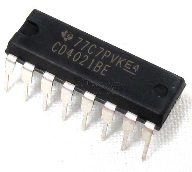


CD4021BE are 8-stage parallel- or serial-input/serial output registers having common CLOCK and PARALLEL/SERIAL CONTROL inputs, a single SERIAL data input, and individual parallel “JAM” inputs to each register stage. Each register stage is D-type, master-slave flip-flop.
- Medium speed operation…12 MHz (typ.) clock rate at VDD – VSS = 10 V
- Fully static operation
- 8 master-slave flip-flops plus output buffering and control gating
- 100% tested for quiescent current at 20 V
- Maximum input current of 1 µA at 18 V over full package-temperature range; 100 nA at 18 V and 25°C
- Noise margin (full package-temperature range) =
1 V at VDD = 5 V
2 V at VDD = 10 V
2.5 V at VDD = 15 V - Standardized, symmetrical output characteristics
- 5-V, 10-V, and 15-V parametric ratings
- Meets all requirements of JEDEC Tentative Standard No. 13B, “Standard Specifications for Description of ’B’ Series CMOS Devices”
- Applications:
- Parallel input/serial output data queueing
- Parallel to serial data conversion
- General-purpose register
Be the first to review “8-stage shift register – CD4021BE”
You must be logged in to post a review.
Related products




Reviews
There are no reviews yet.