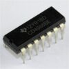
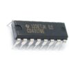
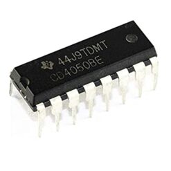
8-Channel multiplexer – CD4051BE
0.150ر.ع.
1 in stock
SKU: ICM-00032
Categories: ICs, Integrated Circuits (ICs) & Modules
The CD4051BE is an analog multiplexer digitally-controlled analog switches having low ON impedance and very low OFF leakage current. These multiplexer circuits dissipate extremely low quiescent power over the full VDD – VSS andVDD – VEE supply-voltage ranges, independent of the logic state of the control signals.
- Wide Range of Digital and Analog Signal Levels
- Digital: 3 V to 20V
- Analog: ≤ 20VP-P
- Low ON Resistance, 125 Ω (Typical) Over 15 VP-P Signal Input Range for VDD – VEE = 18 V
- High OFF Resistance, Channel Leakage of
±100 pA (Typical) at VDD – VEE = 18 V - Logic-Level Conversion for Digital Addressing Signals of 3 V to 20 V (VDD – VSS = 3 V to 20 V) to Switch Analog Signals to 20 VP-P (VDD – VEE = 20 V) Matched Switch Characteristics, rON = 5 Ω (Typical) for VDD – VEE = 15 V Very Low Quiescent Power Dissipation Under All Digital-Control Input and Supply Conditions, 0.2 µW (Typical) at
VDD – VSS = VDD – VEE = 10 V - Binary Address Decoding on Chip
- 5 V, 10 V, and 15 V Parametric Ratings
- 100% Tested for Quiescent Current at 20 V
- Maximum Input Current of 1 µA at 18 V Over Full Package Temperature Range, 100 nA at 18 V and 25°C
- Break-Before-Make Switching Eliminates Channel Overlap
Be the first to review “8-Channel multiplexer – CD4051BE” Cancel reply
You must be logged in to post a review.





Reviews
There are no reviews yet.