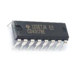
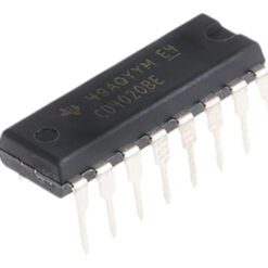
Triple 3-Input AND Gate (CD4073BE )
0.200ر.ع.
Out of stock
SKU: ICM-00055
Categories: ICs, Integrated Circuits (ICs) & Modules
CD4073BE AND gates, provide the system designer with direct implementation of the AND function and supplement the existing family of CMOS gates.
Features:
- Medium-Speed Operation – tPLH, tPHL = 60 ns (typ.) at VDD = 10 V
- 100% tested for quiescent current at 20 V
- Maximum input current of 1 µA at 18 V over full package-temperature range: 100 nA at 18 V and 25°C
- Noise margin (full package-temperature range) =
- 1 V at VDD = 5 V
- 2 V at VDD = 10 V
- 2.5 V at VDD = 15 V
- Standardized, symmetrical output characteristics
- 5-V, 10-V, and 15-V parametric ratings
- Meets all requirements of JEDEC Tentative Standard No. 13B, “Standard Specifications for Description of ‘B’ Series CMOS Devices”
Be the first to review “Triple 3-Input AND Gate (CD4073BE )” Cancel reply
You must be logged in to post a review.


Reviews
There are no reviews yet.