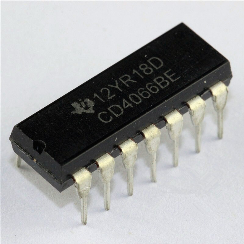
Quad Bilateral Switch – CD4066BE
0.150ر.ع.
5 in stock
SKU: ICM-00033
Categories: ICs, Integrated Circuits (ICs) & Modules
The CD4066BE device is a quad bilateral switch intended for the transmission or multiplexing of analog or digital signals.
- 15-V Digital or ±7.5-V Peak-to-Peak Switching
- 125-Ω Typical On-State Resistance for
15-V Operation - Switch On-State Resistance Matched to Within
5 Ω Over 15-V Signal-Input Range - On-State Resistance Flat Over Full
Peak-to-Peak Signal Range - High On or Off Output-Voltage Ratio:
80 dB Typical at fis = 10 kHz, RL = 1 kΩ - High Degree of Linearity: <0.5% Distortion Typical at fis = 1 kHz, Vis = 5-Vp-p
VDD – VSS ≥ 10-V, RL = 10 kΩ - Extremely Low Off-State Switch Leakage, Resulting in Very Low Offset Current and High Effective Off-State Resistance: 10 pA Typical at VDD – VSS = 10-V, TA = 25°C
- Extremely High Control Input Impedance
(Control Circuit Isolated From Signal Circuit):
1012 Ω Typical - Low Crosstalk Between Switches: –50 dB Typical at fis = 8 MHz, RL = 1 kΩ
- Matched Control-Input to Signal-Output Capacitance: Reduces Output Signal Transients
- Frequency Response,
Switch On = 40 MHz Typical - 100% Tested for Quiescent Current at 20-V
- 5-V, 10-V, and 15-V Parametric Ratings
Be the first to review “Quad Bilateral Switch – CD4066BE” Cancel reply
You must be logged in to post a review.


Reviews
There are no reviews yet.